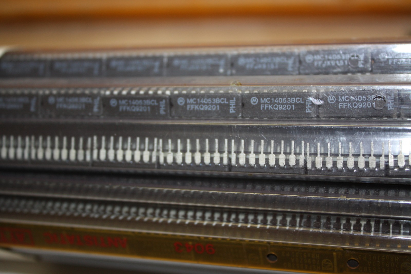
The MC14051B, MC14052B, and MC14053B analog multiplexers are digitallycontrolled analog switches. The MC14051B effectively implements an SP8T solid state switch, the a DP4T, and the MC14053B a Triple SPDT. All three devices feature low ON impedance and very low OFF leakage current. Control of analog signals up to the complete supply voltage range can be achieved. Triple Diode Protection on Control Inputs Switch Function is Break Before Make Supply Voltage Range = 3.0 Vdc to 18 Vdc Analog Voltage Range (VDD VEE) 18 V Note: VEE must be VSS Linearized Transfer Characteristics Lownoise 12 nV/Cycle, f 1.0 kHz Typical PinforPin Replacement for CD4051, CD4052, and CD4053 For 4PDT Switch, See MC14551B For Lower RON, Use the or HC4053 HighSpeed CMOS Devices
Symbol VDD Parameter Value Unit V DC Supply Voltage (Referenced to VEE, VSS VEE) + 18.0 Vin, Vout Iin Input or Output Voltage (DC or Transient) (Referenced to VSS for Control Inputs and VEE for Switch I/O) Input Current (DC or Transient), per Control Pin Switch Through Current Storage Temperature 0.5 to VDD V mA Isw PD Power Dissipation. per Package mW Tstg + 150
TL Lead Temperature (8Second Soldering) _C * Maximum Ratings are those values beyond which damage to the device may occur. Temperature Derating:”P and D/DW” Packages: 7.0 mW/_C From To 125_C Ceramic “L” Packages: 12 mW/_C From To 125_C
Note: Control Inputs referenced to VSS, Analog Inputs and Outputs reference to VEE. VEE must be VSS.


Recensioni
Ancora non ci sono recensioni.